From a System-Level to a Device-Level Simulation of a Buck Converter
The primary goal of the following example is to demonstrate the suitability of SIMBA for performing simulations at the system and device level. For this purpose a simple buck converter in an open loop is used.
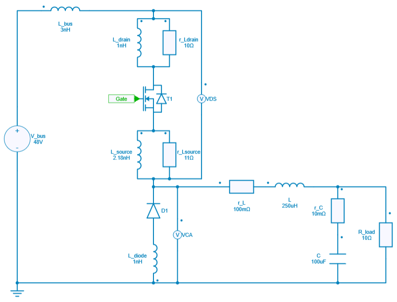
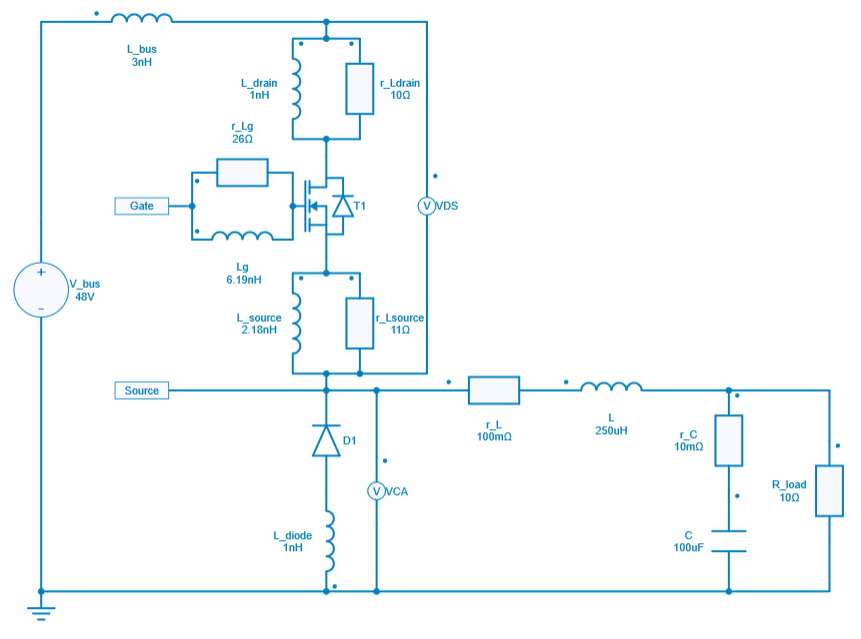
Electrical Circuit
The analysis includes the following scenarios with the model of the buck converter:
-
Simulation using ideal switches:
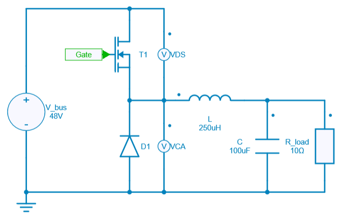
-
Simulation using ideal switches along with parasitic components:
-
Simulation with detailed switch models along with parasitic components:
MOSFET and Diode model
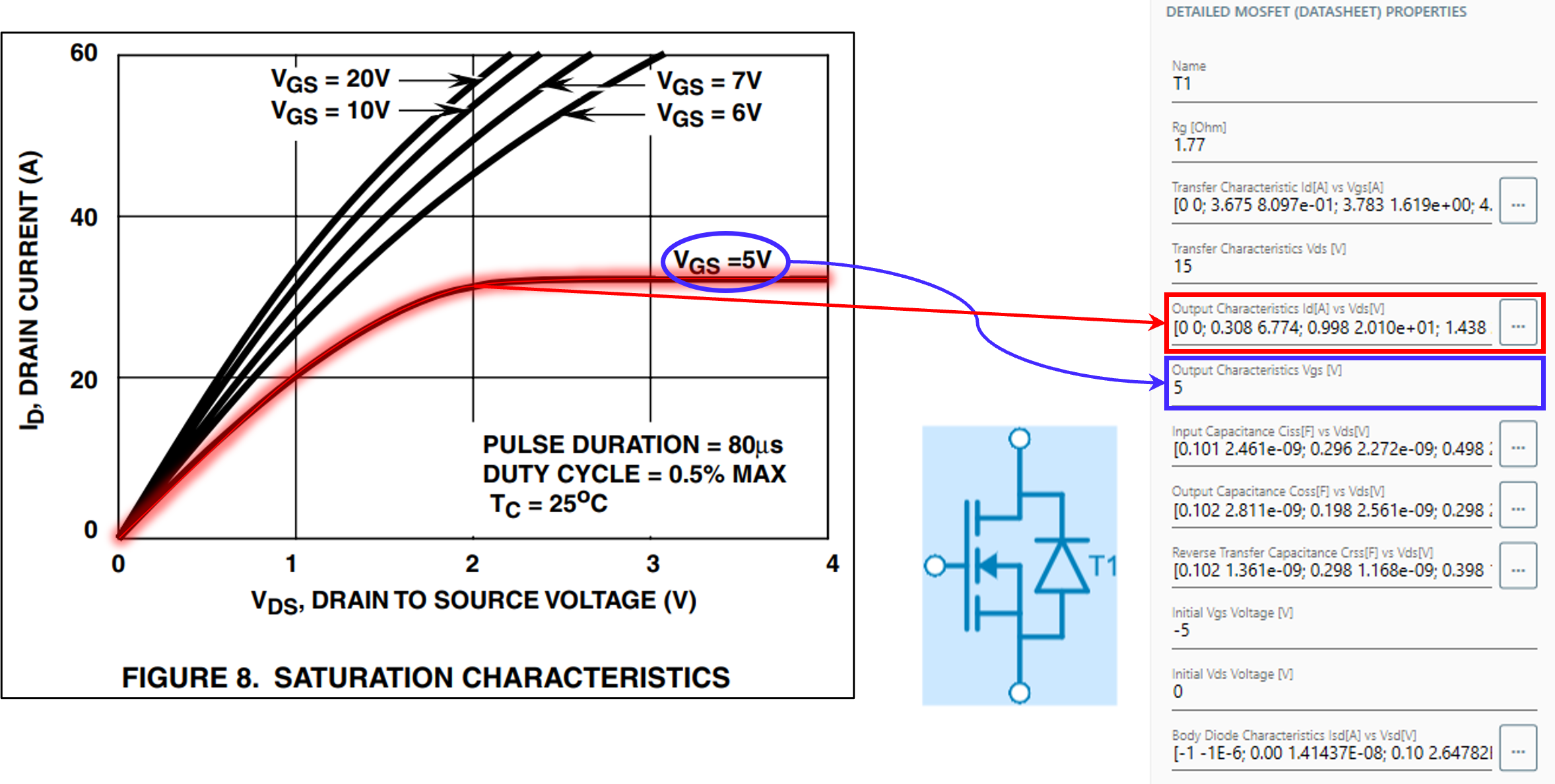
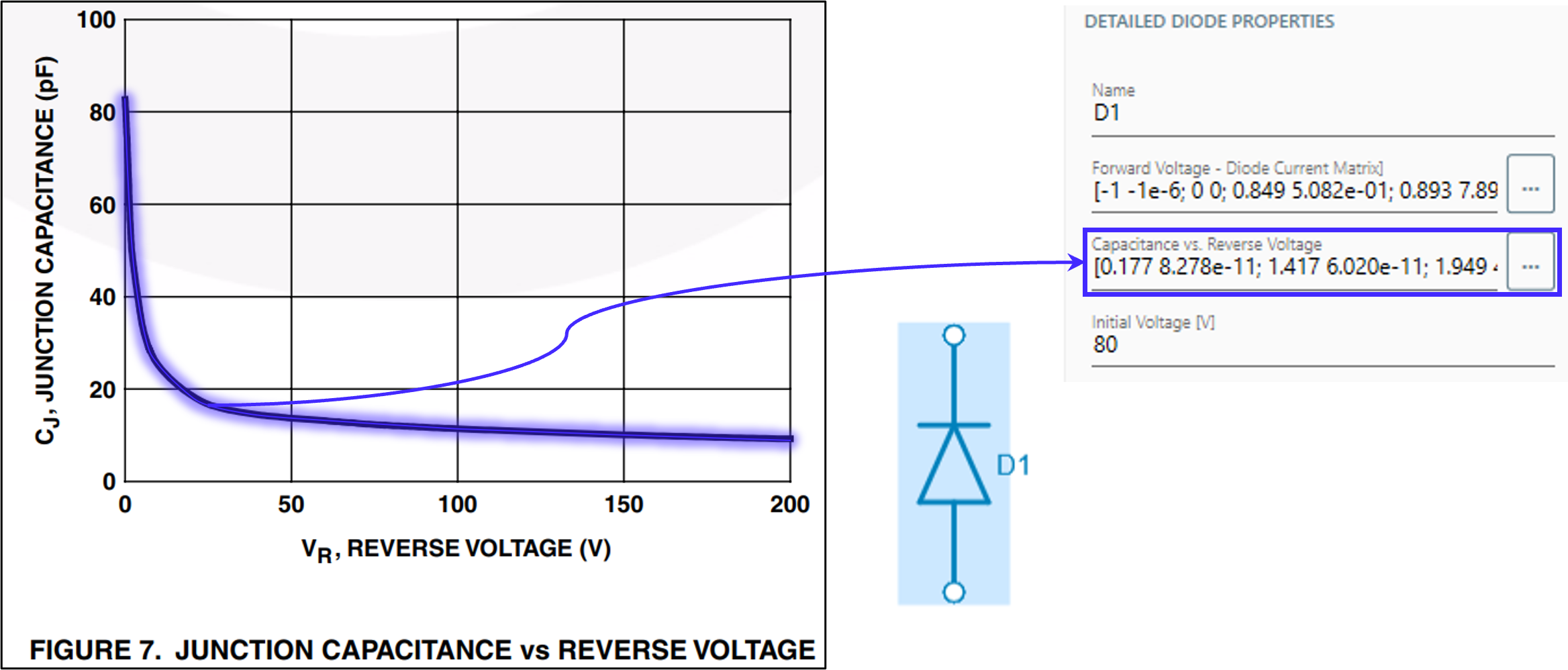
Using the datasheet provided by the manufacturer, we can extract the most critical characteristics used to model both the diode and the transistor, and then insert them into SIMBA. The data can be easily extracted from the datasheet using a tool such as WebPlotDigitizer.
The following figures show example curves extracted from the datasheet of a given component and imported into SIMBA:
-
Extraction of the output (saturation) characteristics of the MOSFET:
-
Extraction of the junction capacitance of the diode:
Parasitic components
For this particular transistor, the manufacturer has provided a PSPICE model in the datasheet that includes both code and a graphical representation of the subcircuit that characterizes the model. This allowed us to extract the parasitic components of the terminals of the transistor, resulting in a more accurate behavior of the model that is aligned with the manufacturer's design. This is shown in the figure below:
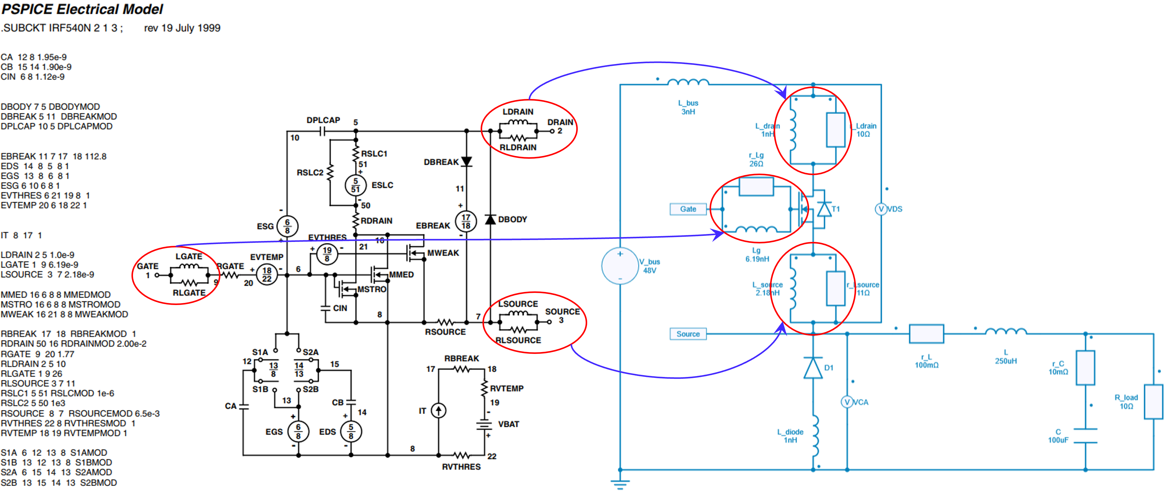
It's worth noting that this approach differs from the traditional method of introducing parasitics, such as implementing Equivalent Series Resistance (ESR) of an inductor. In this example, we have directly adopted the manufacturer's approach by including the inductance in parallel with the resistor.
In addition to the parasitic components of the MOSFET terminals, we have also included the parasitic inductance of the bus and diode, as well as the ESR of the capacitor and inductor in the LC filter.
Control Circuit
The control circuit for the first two cases in which the ideal switches have been used is shown in the following figure:
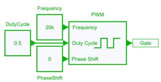
In the first two examples where ideal transistors are used, a Controlled PWM Generator block is used to generate an ideal square wave at its output, allowing the user to set the rise and fall times and other basic parameters such as frequency, duty cycle and phase shift.
For the third example of a buck converter where a detailed transistor model is used an electrical control signal is required. Therefore, it is necessary to convert the control signal (green) to an electrical (blue) signal with an amplitude exceeding threshold voltage of the transistor to ensure its full turn-on. To achieve this, the following gate driver circuit was used:
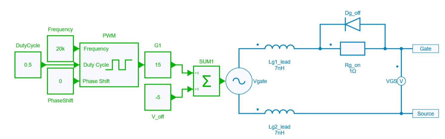
In the case of the control circuit for the detailed MOSFET model, the control signal is first generated by the PWM block. The binary signal is then amplified with a gain of 15 and a value of 5 is subtracted. The control signal is then fed to the controlled voltage source, where the control values are converted to voltage. This process results in a high signal of 10 V and a low signal of -5 V.
To replicate the effects of unwanted long wires feeding the control signal to the gate, parasitic inductances were implemented in the gate driver circuit. Additionally, a Dg_off diode was employed to speed up the transistor's turning-off process.
Results
Start-up Transient State
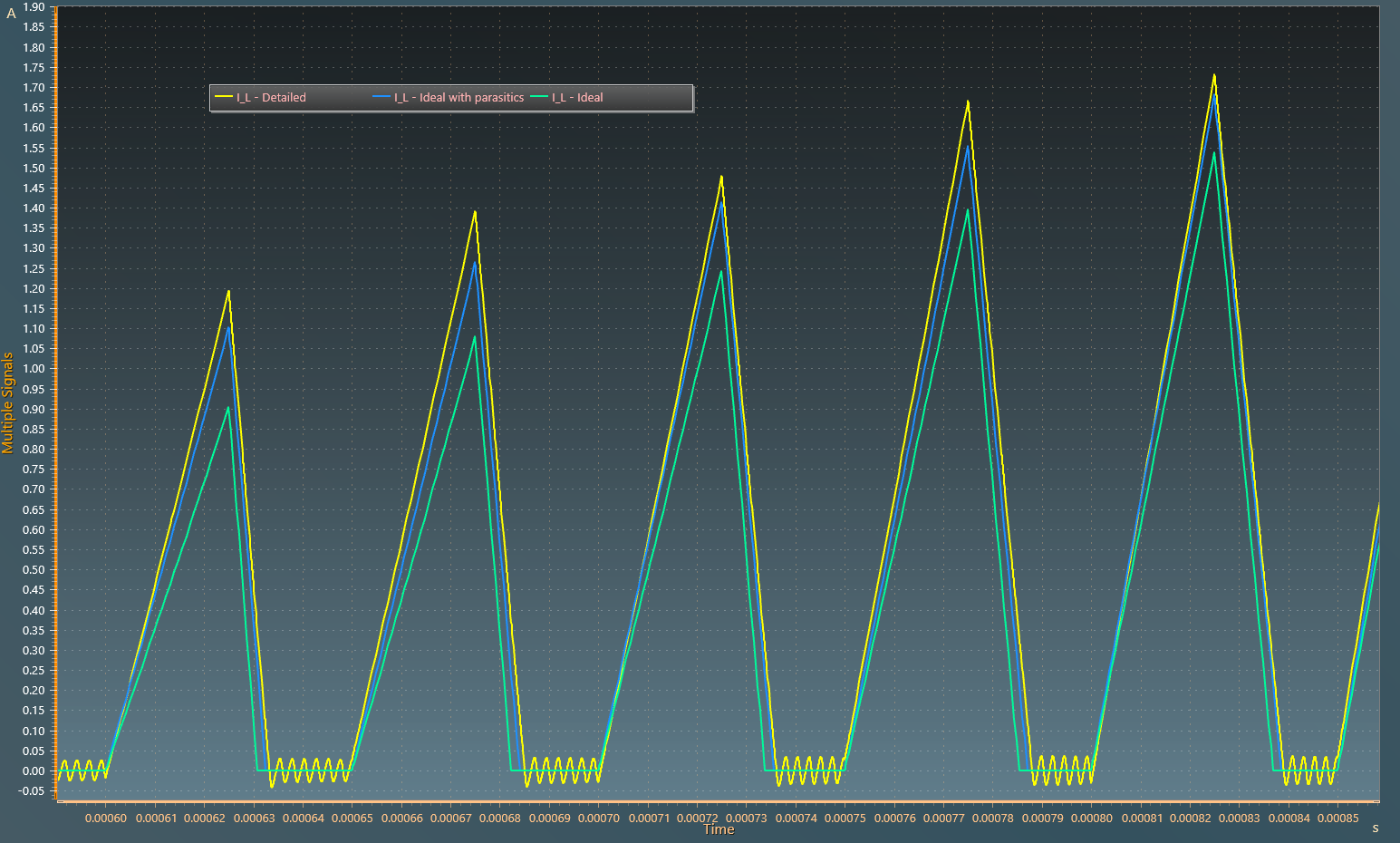
The current flowing through the inductor is shown in the figure below:
The voltage across the drain and source of the MOSFET, zoomed in on the oscillation as the transistor turns off, is shown in the figure below:
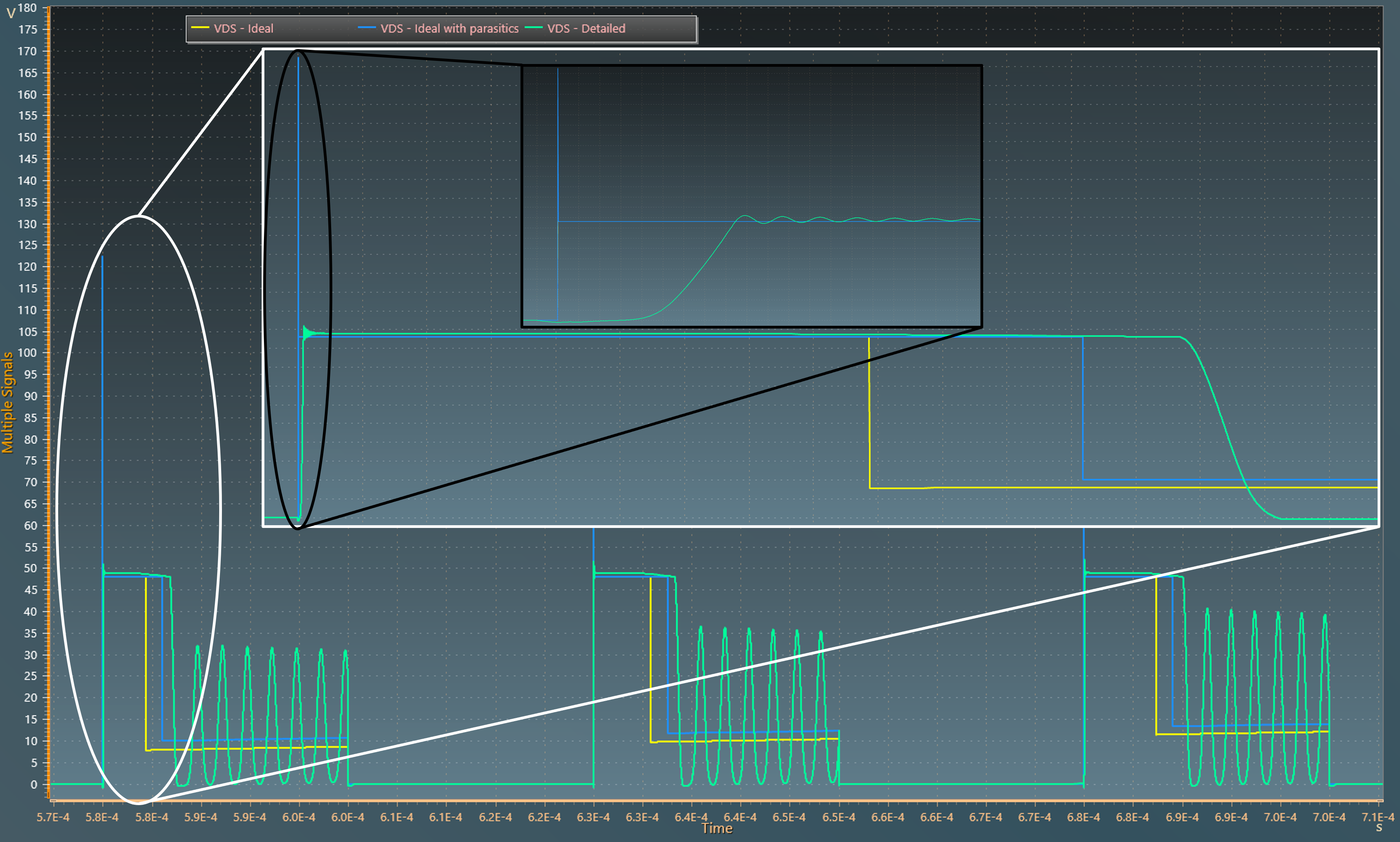
From the analysis of the figures above, it can be seen that during the transient state, the buck converter is in discontinuous conduction mode (DCM) as the inductor is being completely discharged. Additionally, during the off time, we can observe an oscillation caused by the parasitic capacitances of the diode and MOSFET, along with the buck converter's inductor forming an LC tank circuit.
Steady State
The figure below shows a magnified view of the current flowing through the diode during the turn-on and turn-off transients:
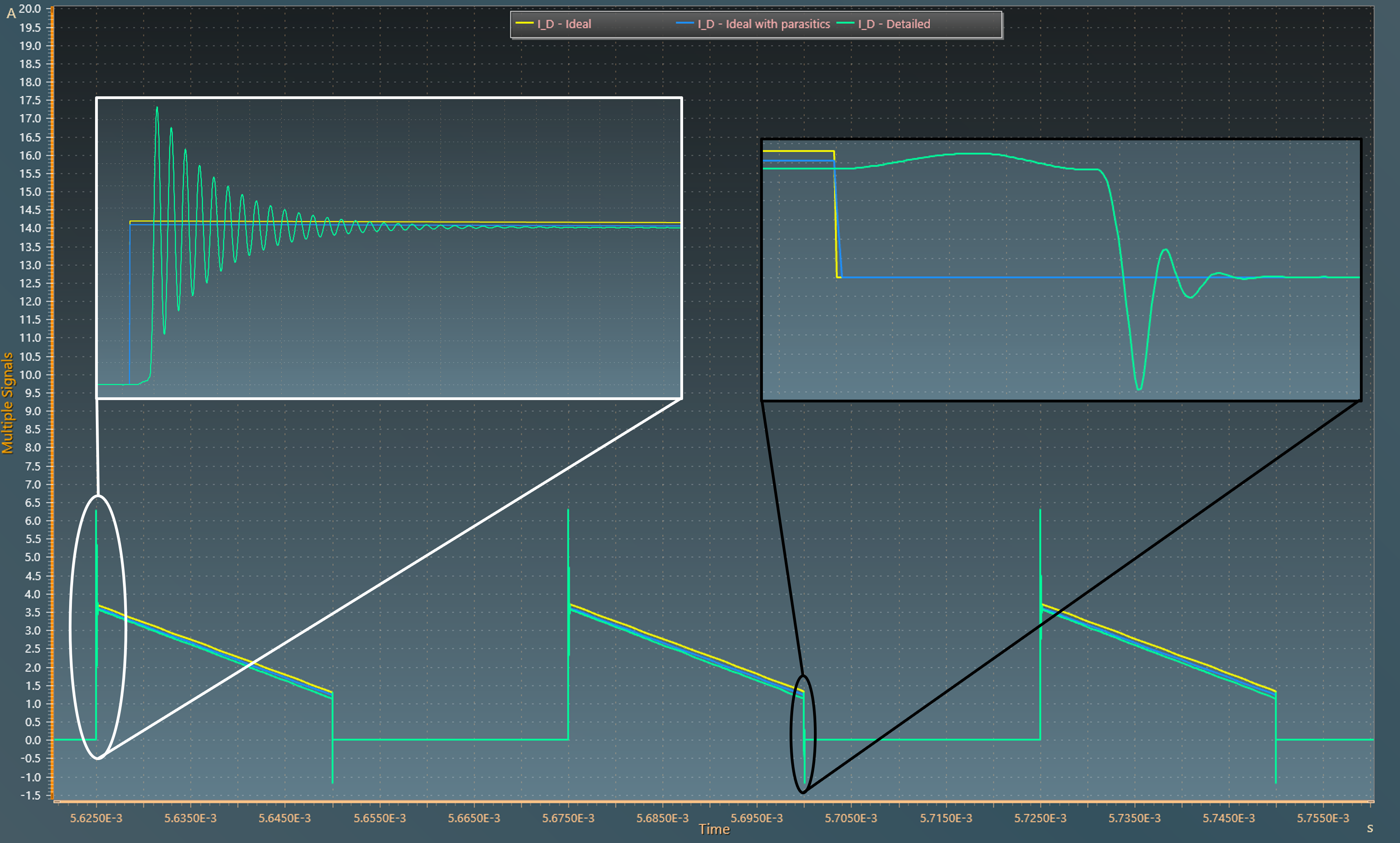
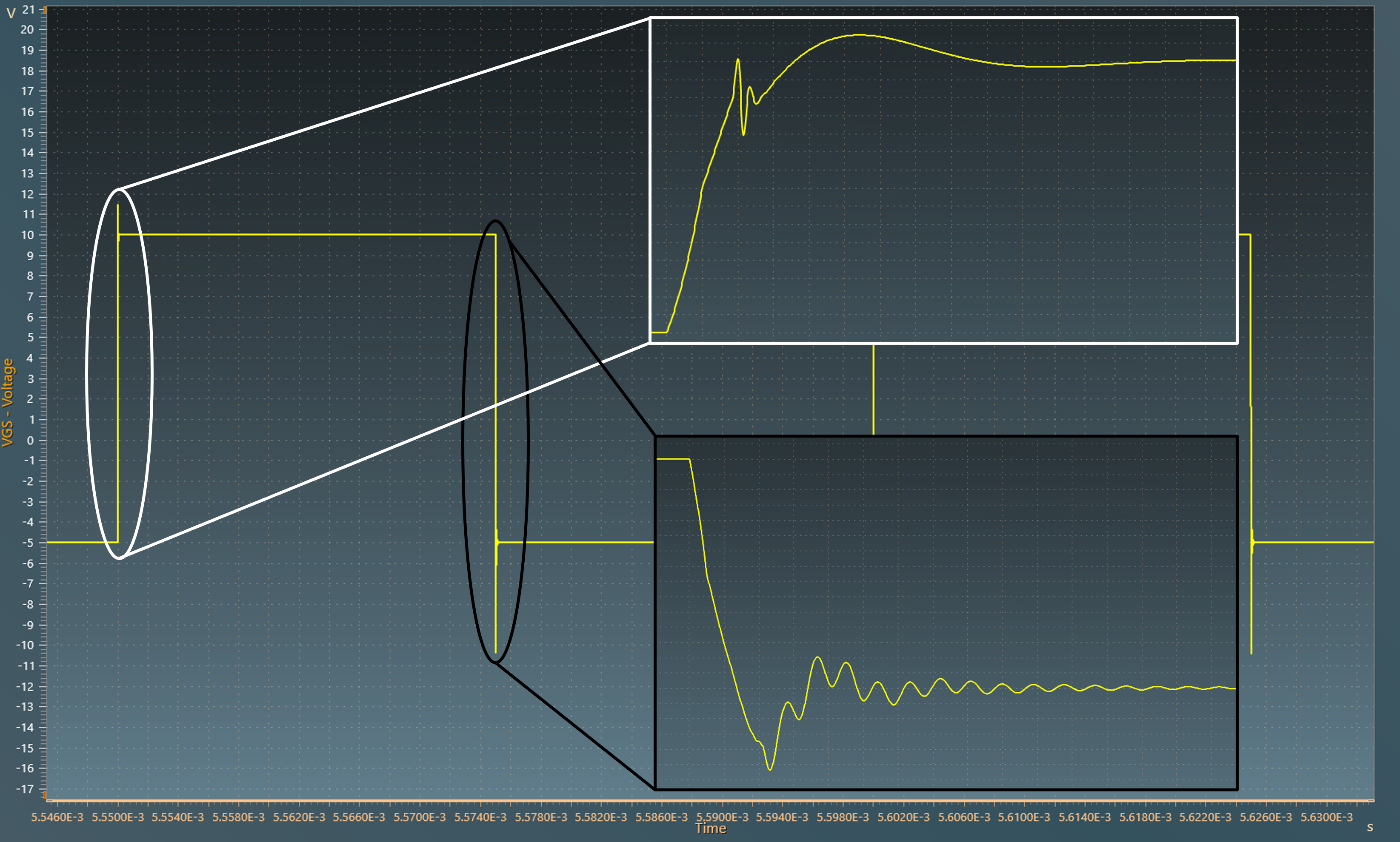
The detailed model of the MOSFET allows the observation of various phenomena, such as the Miller plateau. Furthermore, the implementation of lead inductances creates an LC tank with the gate-source capacitance, causing visible oscillations as demonstrated in the figure below:
Conclusion
This example shows how SIMBA can handle a variety of simulation complexities, from idealized system representations to more complex device-level models, making it a useful tool for transient analysis in power electronics.