Single phase PFC with bang-bang control
This example shows an AC-DC Converter with PFC Bang-Bang control technic and having:
- a sinusoidal input peak voltage of 200 V,
- an output DC voltage reference set at 300 V,
- an average power of around 625 W transferred at the output resistor.
PFC with bang-bang control provide some advantages:
- higher power than conventionnal L&C filter (until KW),
- a cost relatively low for a comparator,
- a simple control to implement,
- an increase of the overall efficiency of the power converter,
- an active PFC offers superior power factor performance with little degradation over a wide operating range,
- the primary benefits of a PFC converter are a high power factor and low Total Harmonic Distorsion (THD).
Model
Model can be downloaded here.
The figure below shows the model of this circuit:
- the first part is composed of a single phase diode bridge to rectify the input signal with an average value of 127.21 V at voltage probe VP1.
- the second part is composed of the "PFC Bang-Bang" - here a boost converter and its hysteresis controller - with a controller for the output DC voltage.
Note
The boost converter has become the dominant PFC topology because the input inductor prevents high di/dt, making the topology better equipped to achieve low input current distortion. The boost inductor with PFC usually operates the converter in continuous conduction mode (CCM), which effectively reduces the input current harmonics.
The bang-bang technique is illustrated by the "hysteresis comparator": the rectified voltage VP1 is normalized, multiplied with the current reference from the voltage controller and then compared with the current through the inductor. The hysteresis value of 0.5 A is set. Finally, the output of this comparator will control the power switch.
Following parameters are considered for the power switches:
- bridge diodes: V_d~=~0.2~V and R_d =~10~m\Omega,
- boost mosfet: R_{on}~=~60~m\Omega and boost diode: V_d~=~0.1~V and R_d =~30~m\Omega.
Here are the values of the other components:
- grid inductor: Lgrid = 30 uH,
- boost inductor L1: 500 uH and initial current of 0 A,
- boost capacitor C1: 2 mF and initial voltage of 0 V,
- load resistor R1: 144 Ω.
The output DC voltage reference is set at 300 V.
Important
As a boost converter is only capable of stepping up its input voltage, the regulated output voltage of the PFC converter must be greater than the peak input voltage.
Simulation
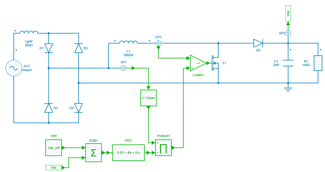
The first figure below shows the rectified voltage across VP1 with a peak voltage \hat{V_{in}} of 200 V.
Typical values such as (V_{P1})_{rms} or (V_{P1})_{average} can be be computed as below and checked with results on the graph (average and rms values are displayed at the right bottom of the graph):
-
(V_{P1})_{rms} = \dfrac {\hat{V_{in}}}{\sqrt{2}} = \dfrac {200 }{\sqrt{2}} = 141.42~V
-
(V_{P1})_{average} = \dfrac {2 \times \hat{V_{in}} }{\pi} = \dfrac {2 \times 200 }{\pi} = 127.32~V
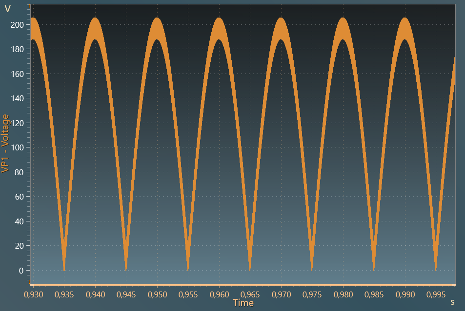
The second figure below shows the output DC voltage regulated at 300 V, with a residual voltage ripple of 3.3 V, which represents around 1.1% of the reference voltage.
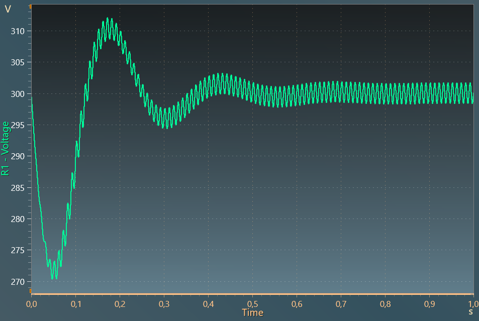
The last figure below shows input current and voltage which are well in phase.
The total harmonic distorsion has been computed with the first 100 current harmonics from the 50 Hz fundamental and shows a value of around 1.94 %.
Power Factor(s) and Total Harmonic Distorsion
Power factor (PF) is usually defined as the ratio between the real power measured in Watts (W) consumed by a load divided and the total apparent power measured in Volt-Amps (VA) circulating between the power source and load.
In AC systems with linear loads, the power factor is a displacement power factor (DPF) and is linked with a measure of the relative difference of phase (\varphi) between the voltage and current signals transferred to the load:
For non-linear loads, i.e. with non-sinusoïdal currents, a distorsion power factor has also to be considered:
where THD_i is the total harmonic distorsion of the current defined by:
The result when multiplied with the displacement power factor previously introduced with linear loads leads to the overall power factor:
For an electronic application that is powered from the AC grid, the input current does not naturally follow the instantaneous AC line voltage and can also be non-sinusoïdal currents which can lead to low power factors.
To address the challenges of phase delay as well as current distortion, a power factor correction stage can be introduced.
Reference
Power Factor Correction (PFC) Circuit Basics, Power Supply Design Seminar by Texas Instruments