Non-Inverting Buck-Boost Converter
This example shows a DC-DC Non-Inverting Buck-Boost Converter with:
- an input voltage of 8 V,
- an output voltage of 24 V (depending on duty cycle {D}),
- a power of 114 W transferred (P_{output} = P_{input}).
A non-inverting Buck-Boost converter is a type of DC-DC converter that can either step up or step down the input voltage to produce a regulated output voltage based on the duty cycle. As the name implies, it does not reverse the polarity of the output voltage, in contrast to a typical buck-boost converter. The power rating of a non-inverting Buck-Boost converter can vary widely depending on the specific application and requirements. It can range from a few watts for low-power portable electronics to several kilowatts for high-power applications such as solar inverters.
Model
In this model, all components are ideal.
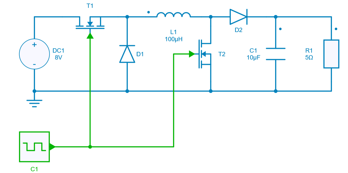
Since this converter is made up of a Buck and a Boost converter connected in series (two switching cells T1, D1 and T2, D2), three main modes of operation can be distinguished:
- Buck mode (T2 is constantly OFF, while T1 is switching) presented in Buck Converter application example,
- Boost mode (T1 is constantly ON, while T2 is switching) presented in Boost Converter application example,
- Buck-Boost mode (T1 and T2 are switched simultaneously).
In this application example we only focus on Buck-Boost operation mode, where both transistors T1 and T2 are switched simultaneously.
When the two switches are closed (ON-state), the input DC voltage source is connected to the inductor L1, causing current to flow. The rising current charges the coil, which stores energy in the form of a magnetic field.
When the two switches are opened (OFF state), the inductor L1 releases stored energy and the current through the inductor begins to decrease. The inductor now acts as an energy source, supplying current to the output capacitor C1 and load resistor R1. The output voltage is therefore regulated by controlling the duty cycle of the two transistors.
Switch control
The switch model can be directly connected with a control signal. For this control, we use a PWM block with an amplitude of 1 and a frequency of 100 kHz.
Here are the values of the other components :
- inductor L1 : 100 µH and initial current = 0 A,
- capacitor C1: 10 µF and initial voltage = 0 V,
- resistor R1: 5 Ω,
- transistor T1: Ron = 0 Ω,
- transistor T2: Ron = 0 Ω,
- diode D1: Rd = 0 Ω and forward voltage = 0 V,
- diode D2: Rd = 0 Ω and forward voltage = 0 V.
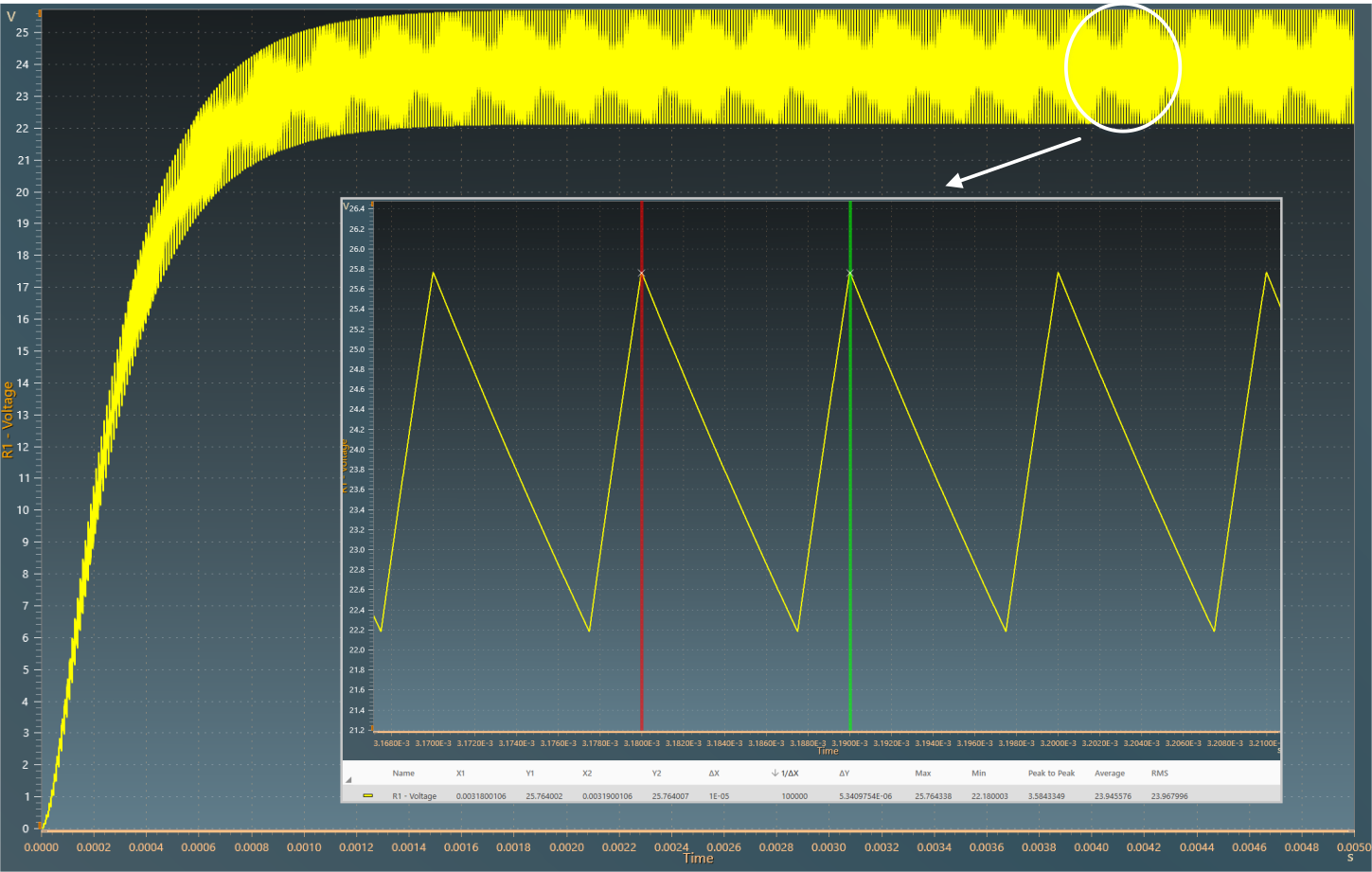
Simulation
The results below show the output voltage across R1 with a duty cycle D = 0.75. A zoom shows a measure of the average value of this voltage : 24 V.
The results below show the output voltage across R1 with a duty cycle D = 0.5. A zoom shows a measure of the average value of this voltage : 8V.
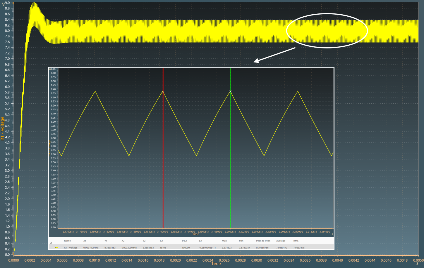
The results follow the equation: V_{out} = V_{in} \times \frac{D}{1-D}
with:
- D : Duty cycle
- V_{in} : Input voltage
- V_{out} : Output voltage