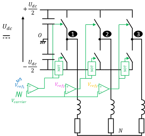
Modulation Strategies for 3-phase 2-Level Voltage Source Inverters
For 3-phase voltage source converters, to increase the DC voltage utilization (i.e. boost the output AC voltage) or reduce the switching losses, a zero-sequence reference can be inserted in the modulation scheme provided the neutral point of the 3-phase system is floating.
info
Modulation depth has a maximal value of 1 in Sine modulation and \sqrt{2/3} \approx 1.15 for other modulation strategies which add a third harmonic component.
This example presents the best of these modulation strategies - in terms of linear range and / or harmonic distortion - which can be easily implemented with C-code or control blocks.
The V_{kO} phase voltage can be given by the equation below, where k = 1, 2, 3:
The V_{NO} voltage is managed with a zero sequence reference voltage.
Thus, the zero sequence reference voltage V_{off} is added to each phase reference V_{ref_k}:
Continuous modulation strategies
Sine modulation (Sine PWM)
With this modulation strategy, the maximum modulation index m_a is equal to 1.
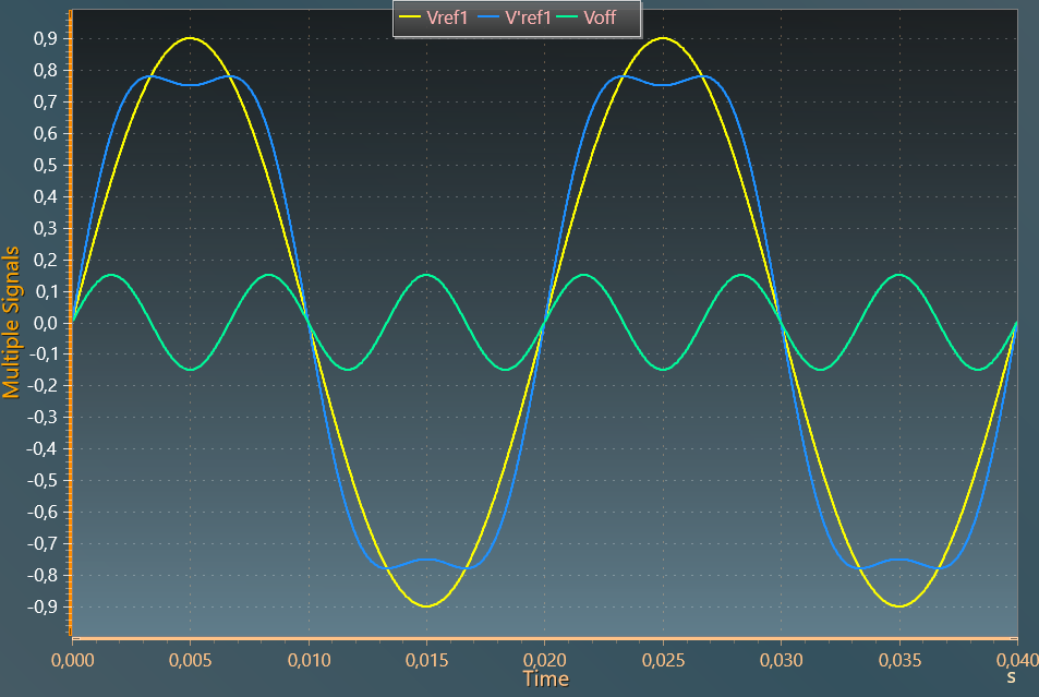
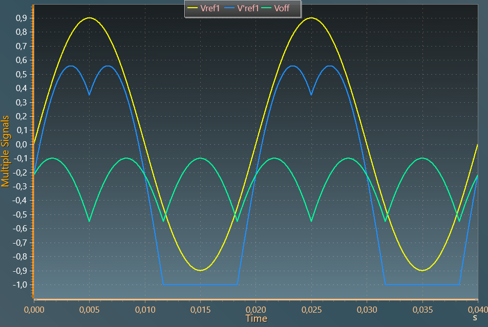
Third-harmonic injection (THIPWM)
This method adds a sinusoidal zero sequence voltage at three-times the fundamental frequency1. This example proposes the implementation of the 1/6 coefficient third-harmonic injection.
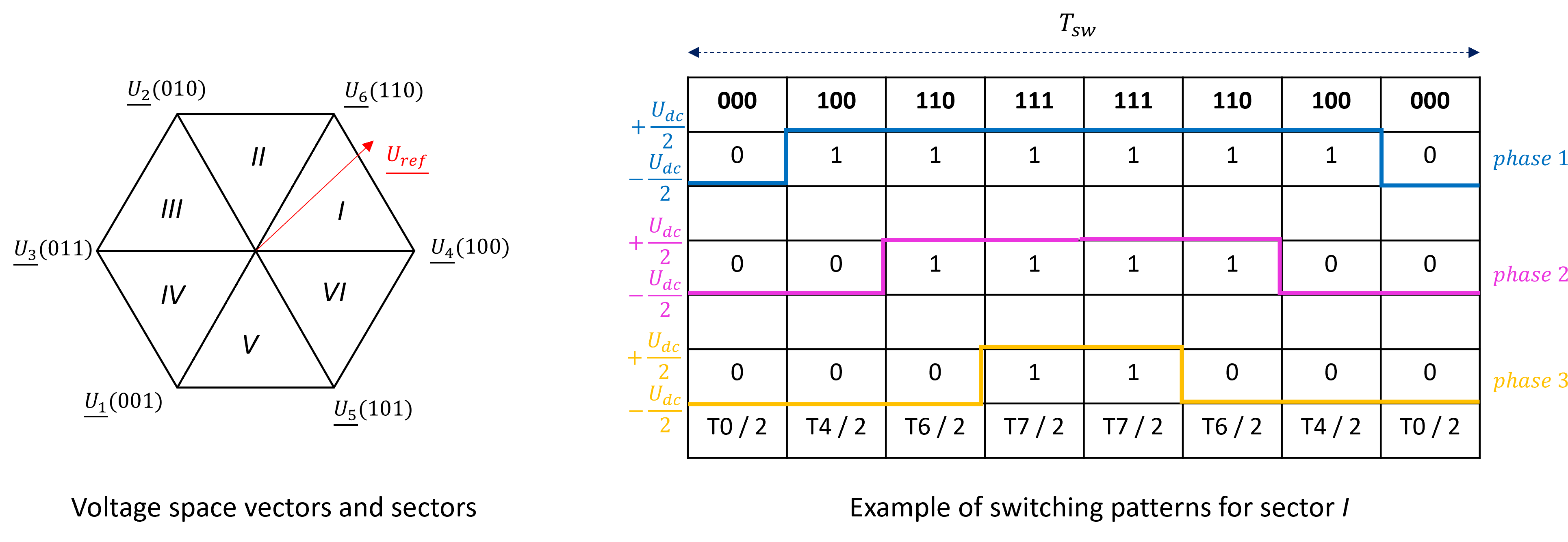
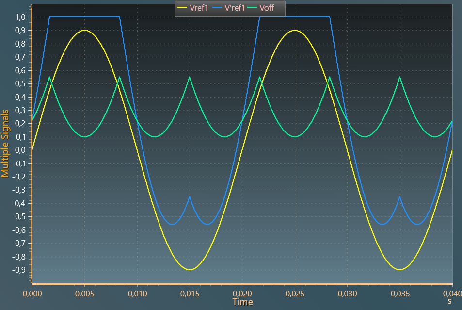
Space vector modulation (SVM)
This modulation strategy is one of the most popular overmodulation methods. It directly defines a sequence of different switching states to follow the complex vector voltage of the three-phase reference system.
The switching pattern of a symmetrical sequence has been implemented in the C-code block.
Caution
It is currently recommended to run this block with the fixed time-step to avoid missing any switching event.
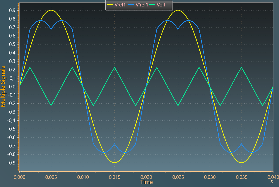
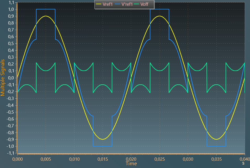
Space vector modulation "carrier based" (SV-PWM)
This modulation strategy offers a similar pattern as the space vector modulation and can be shown as a triangle-intersection or carrier-based implementation of the conventional Space vector modulation 2, 3.
It is also known as the MIN MAX modulation strategy due to the computation of the zero-sequence:
Tip
To get exactly the same swithing pattern as with the conventional SVM, the sampling time of the C-code block which computes the offset voltage must be set at the switching period of the carrier.
Discontinuous modulation strategies
DPWM min
In this strategy, each phase does not switch within 120° of the fundamental period and the output is clamped at the negative dc bus voltage. As consequence, the switches connected to the negative dc bus voltage reduce their switching losses.
DPWM max
In this strategy, each phase does not switch within 120° of the fundamental period and the output is clamped at the positive dc bus voltage. As consequence, the switches connected to the positive dc bus voltage reduce their switching losses.
DPWM1
In this case the phase leg is clamped 30° symmetricaly from maximal voltage. This method has low harmonic distortion characteristics. The zero-sequence is extracted from the following equations:
References
-
G.Buja and G. Indri. “Improvement of pulse width modulation techniques”. Archiv fur Elektrotechnik, 57, pages 281-289, 1975. ↩
-
A.M.Hava, “Carrier based PWM-VSI drives in the overmodulation region”. Vol. 1. University of Wisconsin–Madison, 1998. ↩
-
Ke. Zhou and D. Wang, "Relationship Between Space-Vector Modulation and Three-Phase Carrier-Based PWM: A Comprehensive Analysis", IEEE Transactions On Industrial Electronics, Vol. 49, No. 1, February 2002. ↩