Totem-Pole Bridgeless Boost PFC Converter
This example shows a single-phase totem-pole bridgeless PFC converter for the below operating conditions:
- switching frequency - 100 kHz,
- AC Input Voltage – 240 V, 60 Hz
- Output Voltage – 600 V
- Output Power – 5 kW
Circuit Model
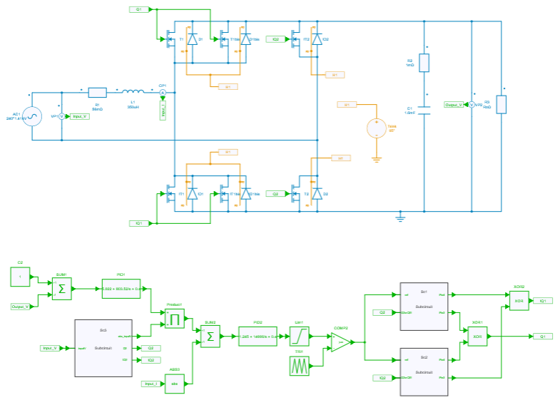
Power Factor Correction control scheme is widely adopted for power conversion of AC-DC application. In this topology, high speed SiC/GaN MOSFETs can be used in the high frequency leg and low resistance silicon MOSFETs can be used in the low frequency leg to improve the efficiency by eliminating the diode drop. The significantly smaller reverse recovery charge of SiC/GaN MOSFETs compared with conventional silicon MOSFETs makes the totem-pole bridgeless PFC practical. It meets the demand for increasing power density of switched-mode power supplies by adopting high switching frequency as well as not to increase switching losses at pulse width modulated (PWM) converters.
The totem-pole bridgeless PFC consists of a pair of SiC/GaN switches that operates at PWM frequency. They work as a pair of boost converters within a half cycle. In either cycle, one SiC/GaN switch will act as a master switch to increase the boost inductor’s current and the other transistor will act as a slave switch to force the current flow to the DC output meanwhile releasing energy. The roles of the pair interchange when AC polarity changes. Also, dead time can be added to avoid the short-circuit of the bridge for SiC/GaN and or Silicon MOSFETs.
Control
The implemented control strategy achieves two main goals:
- to obtain a sinusoidal input current with a unit power factor,
- to regulate output dc voltage.
Hence, two control loops are designed: the inner current control loop and the outer voltage control loop.
PWM modulation
A classical PWM strategy has been implemented with a carrier frequency of 100 kHz.
Inner current control loop
The block diagram of the inner current control loop is represented as below:
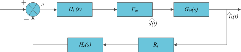
In this control diagram, H_i(s) is the current loop controller, which is designed to maintain the stability of current control loop; G_id(s) is the duty-to-current transfer function; F_m is the pulse-width ratio. R_s is the equivalent sample resistor for unit current. The transfer function of open current loop excluding H_i(s) is:
Also, the transfer function of the current loop controller is:
To have good current loop performance, the bandwidth needs to be within 3~10 kHz, and the phase margin needs to be over 40 degrees.
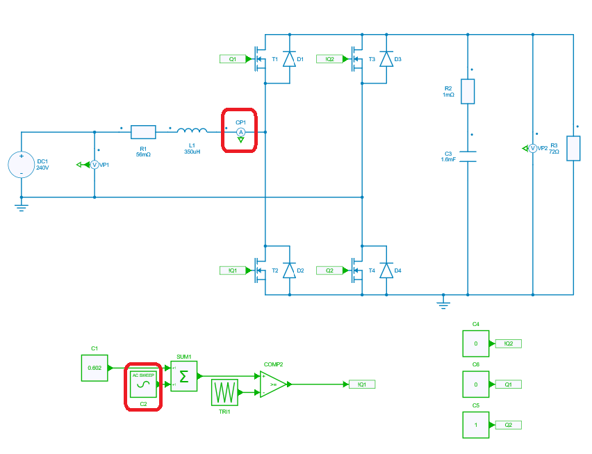
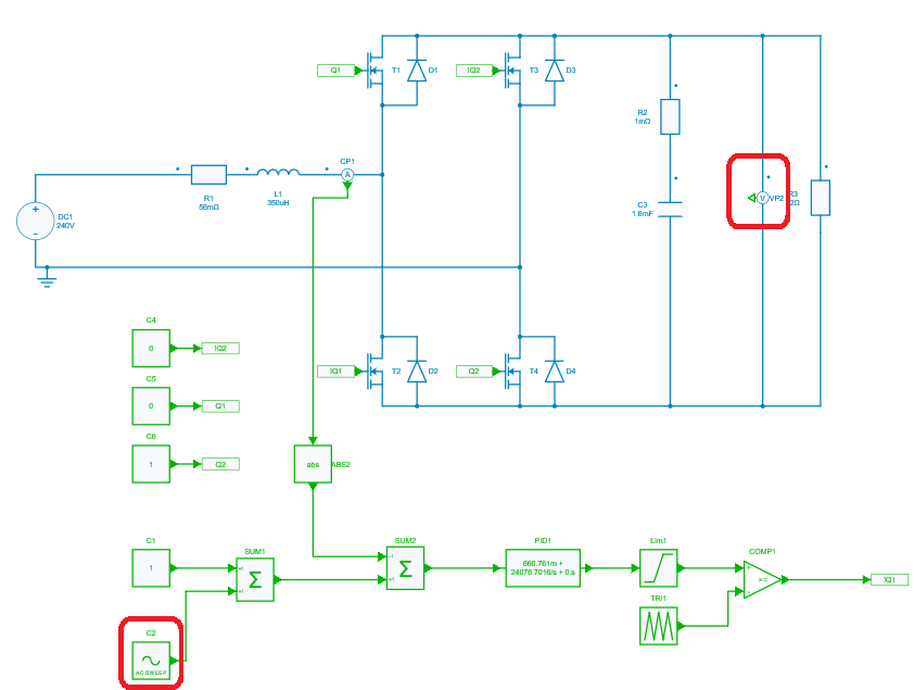
The analysis of bode plot can be done analytically using the above transfer fuction for T_i(s) which can further be used to tune the controller. Alternatively, this transfer function T_i(s) can be plotted using the AC sweep feature with the circuit-setup for inner loop as shown below:
Also, the plot for open-loop transfer function is obtained as below:
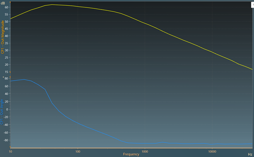
Hence, the bode plot can be used to tune the controller parameters to achieve the required bandwidth and phase margin. In our case, it leads to K_p and K_i coefficients of 0.66 and 24076.7 respectively.
Outer voltage control loop
The overall block diagram for the voltage loop control is shown below:
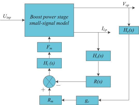
The control-to-output voltage transfer function can be written as:
Here, G_{vd} is the duty-to-output transfer function and g_c = \frac{1}{V_{rms}}.
For the resistive load, the approximated transfer function can be written as:
To have good voltage loop performance, the bandwidth needs to be within 2~15 Hz in order to reduce the effect of input voltage ripple towards inductor current regulation. In this example, the cut-off frequency is set at 12 Hz.
Also, the circuit-setup for outer voltage loop to perform the ac-sweep is as below:
The plot for open-loop transfer function is obtained as below:
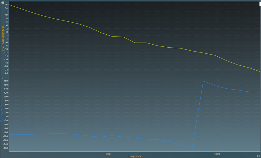
Hence, after performing the ac-sweep and tuning further, the coefficients obtained for K_p and K_i are 5.022 and 803.52 respectively.
Solution for Current Spikes at AC Zero-crossing
There are mainly four scenarios where current spikes can occur 1. That comes from an intrinsic behavior of the Totem Pole converter when the AC voltage is very low after zero crossing. These are discussed as below:
Case-1
When the operation mode changes from negative cycle to positive cycle at the AC zero-crossing, the duty ratio of the upper switch of high frequency leg (Q1) changes abruptly from almost 100 % to zero whereas the duty ration of the lower switch of same leg(!Q1) changes from zero to 100 %. Also, because of the slow reverse recovery of the body diode and the large Coss of lower switch of low frequency leg(Q2), the Vds voltage of this switch still equals to the output voltage (600 V). Since this high voltage is applied to the inductor when the !Q1 turns on, a positive current spike is generated. This can be avoided by the soft-start of this switch.
Case-2
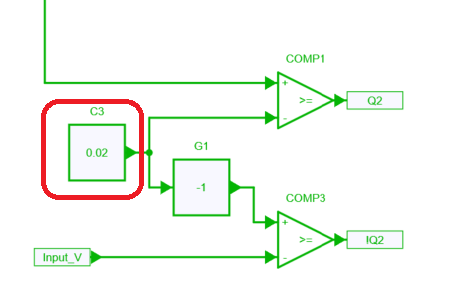
However, even with soft turn on of !Q1, there are still excessive current spikes. This is because input AC voltage is very low right after zero-crossing and is therefore insufficient for the inductor current to build up. On the other hand, when Q1 turns on with 1 – D, even though its duty is not high, the voltage applied to the inductor is high (600 V). The resulting high reverse current through the inductor causes a negative current spike. To avoid this scenario, a dead time between Q2 and !Q2 is introduced which is based on the detection of AC voltage value (2 % of maximum AC voltage in this case) as shown below.
Case-3
If the Q2 turns on before !Q1 soft-start and the body diode of !Q2 is not recovered quickly enough, a shoot-through can occur. Since, the ideal switches are used in the simulation, the solution for this scenario is not required.
Case-4
Now, if Q2 turns on too late, a negative current spike can be generated. The high output voltage (V_{dc}) generates a reverse inductor current when Q1 is on while Q2 is off. This reverse current first turns off the Q2 body diode, then starts to charge C_{oss} of Q2 and hence, the V_{ds} of Q2 builds up to a high voltage. Then, when !Q1 turns on, the high voltage (V_{ds} + V_{in}) that is applied to the inductor results in high rising current in the inductor. Therefore, the inductor’s rising and falling currents are both large magnitude, which achieves a balance that maintains the average current at a small positive value. Now, if Q2 suddenly turns on, as a result, V_{ds} of Q2 will be clamped to zero. Further, if !Q2 turns on, only V_{in} is applied to the inductor. Since V_{in} is very small, which is insufficient for the inductor to build up current high enough, the inductor’s rising current becomes very small. Because the falling current still has a large magnitude, the balance is broken and results in a large negative current spike.
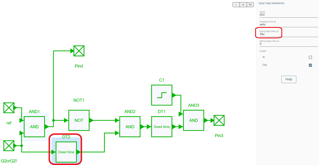
Although, the MOSFETs in the simulation are of ideal in nature, some of the issues are still prevalent. Hence, to avoid the current spikes at zero-crossing and for the simulation to converge, soft start for the high frequency MOSFET is introduced which will conduct the reverse current (for example, Q1 when AC voltage is positive) with a dead-time block as shown below.
Thermal Model
The 4th design of the project includes a thermal description of the SiC Mosfet with the third generation SiC MOSFETs (C3M0075120K) from Wolfspeed. These descriptions are used both in high-frequency switching and low-frequency switching legs. Yet, two mosfets are used in parallel for the high-frequency switching leg.
Simulation Results
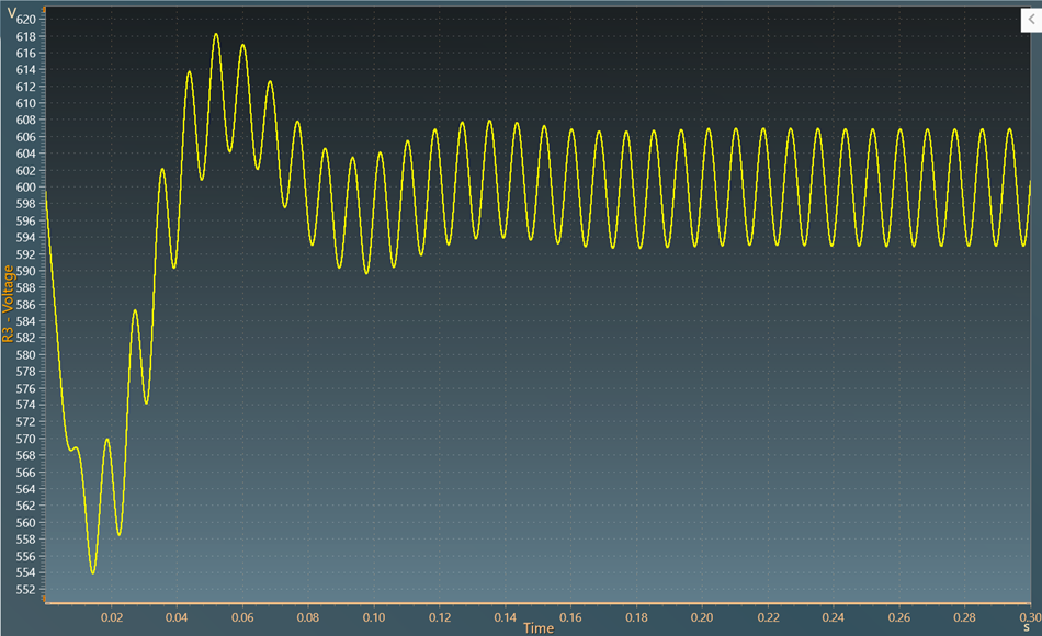
The overall converter can be simulated now and results can be verified. The regulated output voltage is shown below:
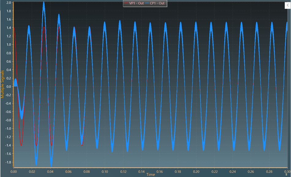
Also, the normalized input voltage and current is obtained as below:
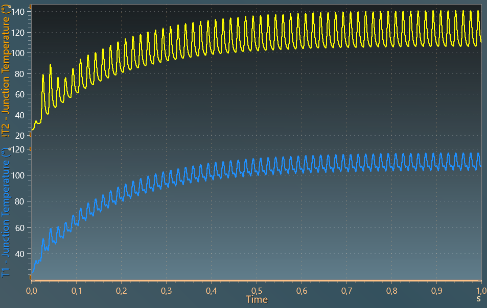
Further, the junction temperatures of the switches T1 and !T2 respectively, can be seen in the result below:
A python notebook has also been written to compute the power factor and the THD of the current and can be downloaded here. In our case, this leads to a power factor of 99.993 % and a THD of 3.14 %.
Reference
[1] Totem-Pole Bridgeless PFC Design Using MC56F82748, Design Reference Manual, NXP Semiconductors, Rev. 0, 11/2016.
-
How to reduce current spikes at AC zero-crossing for totem-pole PFC, by Bosheng Sun, Texas Instruments, Analog Applications Journal, Communications, 2015. ↩