Detailed MOSFET (Datasheet)
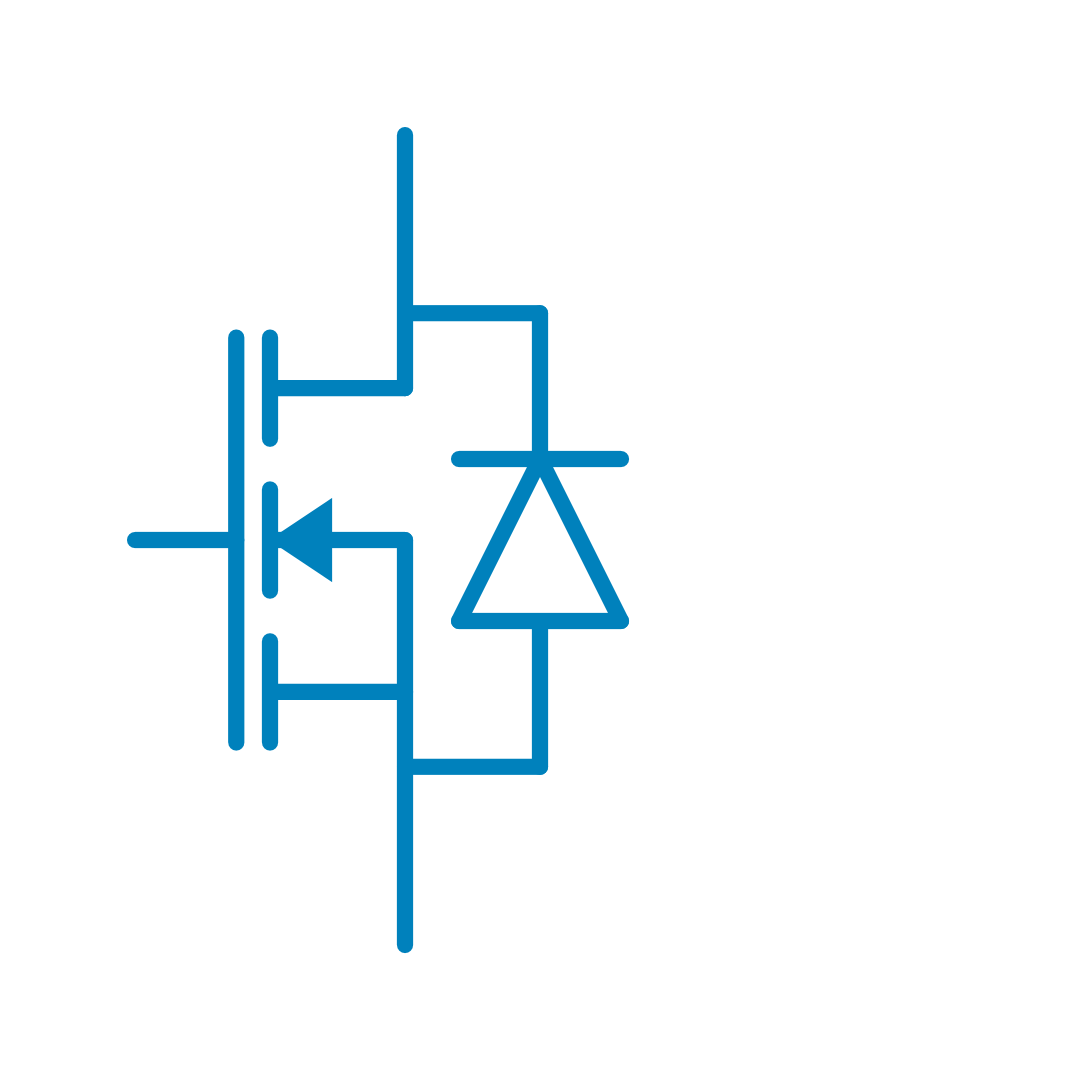
Description
This MOSFET model is developped with two key objectives:
- Accuracy and Computational Efficiency: The model accurately simulates both switching and static behaviors of MOSFETs and is optimized for fast simulation.
- Robustness and Characterization: It is designed to be robust and can be easily characterized using standard datasheet.
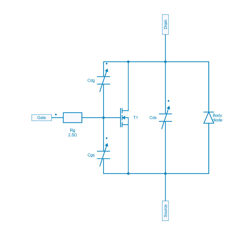
This MOSFET model incorporates:
- Three nonlinear capacitances C_{GD} , C_{GS} , and C_{DS} characterized by Capacitance- V_{DS} matrices, modeling C_{ISS} , C_{OSS} , and C_{RRS} respectively.
- A PWL Diode representing the MOSFET body diode, characterized by a Voltage-Current data matrix.
- An internal piecewise linear MOSFET model using 3D Triangular meshing for output and transfer characteristics (details below).
- An internal gate resistance R_G .
Capacitances
The capacitances are calculated as follows:
Capacitance Consistency
It is recommended that all three capacitances share the same V_{DS} values. If not, interpolation is used to calculate missing V_{DS} values.
Capacitance Options
Alternatively, a single capacitance value can be used to model a V_{DS} -independent capacitance.
Body Diode
To accurately model the diode's off state, include at least one data point with a negative voltage in the characteristics matrix. In most cases, modeling avalanche breakdown is unnecessary.
MOSFET Equations
The internal MOSFET model employs the following drain current equations:
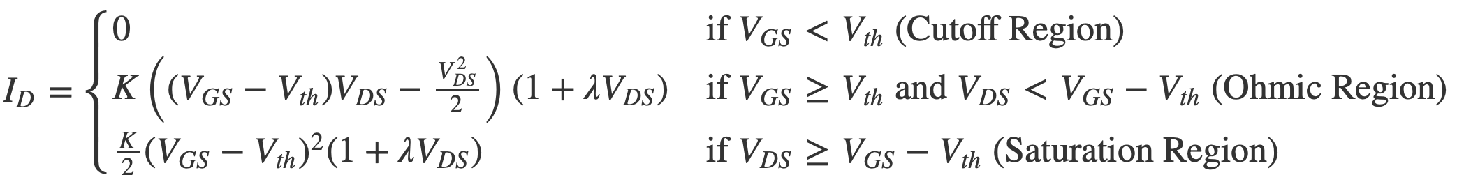
Optimization techniques are employed to derive V_{th} , \lambda , and K from the output and transfer characteristics data. DIRECT (DIviding RECTangles) algorithm is used for this optimization, as described in:
- D. R. Jones, C. D. Pertunen, and B. E. Stuckmann, "Lipschitzian optimization without the lipschitz constant," J. Optimization Theory and Applications, vol. 79, p. 157 (1993).
Initialization
Initial Vds and Vgs values can be set to avoid unphysical current values at t=0.
Library
Electrical > Semiconductors
Pins
| Name | Description |
|---|---|
| Drain | Drain |
| Source | Source |
| Gate | Gate (Control Input) |
Parameters
| Name | Description |
|---|---|
| Rg | Gate Internal Resistance value, in Ohm |
| VgsIdMatrix | Transfer Characteristic |
| VgsIdMatrix_Vds | Transfer Characteristics Vds |
| VdsIdMatrix | Output Characteristics |
| VdsIdMatrix_Vgs | Output Characteristics Vgs |
| Ciss | Input Capacitance, in F |
| Coss | Output Capacitance |
| Crss | Reverse Transfer Capacitance |
| VgsInit | Initial Cgs Capacitor Voltage, in V |
| VdsInit | Initial Cds Capacitor Voltage, in V |
| Vsd_Is_BodyDiodeMatrix | Source Drain current vs Source-Drain Voltage (Body Diode) |